Характеристики
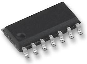
DS90LV019TM/NOPB, LVDS драйвер / ресивер 100Mbps [SOIC-14]The DS90LV019TM is a Driver/Receiver designed specifically for the high speed low power point-to-point interconnect applications. The device operates from a single 3.3 or 5V power supply and includes one differential line driver and one receiver. It features an independent driver and receiver with TTL/CMOS compatibility (DIN and ROUT). The logic interface provides maximum flexibility as 4 separate lines are provided (DIN, DE, RE# and ROUT). The device also features a flow-through pin-out which allows easy PCB routing for short stubs between its pins and the connector. The driver has 3.5mA output loop current. The driver translates between TTL levels (single-ended) to low voltage differential signalling levels. This allows for high speed operation, while consuming minimal power with reduced EMI. In addition, the differential signalling provides common-mode noise rejection.
• LVDS Signalling
• Low power CMOS design
• Balanced output impedance
• Glitch free power up/down (driver disabled)
• High signalling rate capacity (above 100Mbps)
• Ultra low power dissipation
• ±1V Common-mode range
• ±100mV Receiver sensitivity
• Flow-through pin-out
• Industrial temperature range operation
• Green product and no Sb/Br
 Личный кабинет


 Загрузка